UART INTERFACING WITH ARM
UART (Universal Asynchronous Receiver Transmitter) are one of the basic interfaces which provide a cost effective simple and reliable communication between one controller to another controller or between a controller and PC. It demonstrate the principle of UART interfacing with ARM LPC2148 microcontroller.
Synopsis

UART (Universal Asynchronous Receiver Transmitter) are one of the basic interfaces which provide a cost effective simple and reliable communication between one controller to another controller or between a controller and PC. It demonstrate the principle of UART interfacing with ARM LPC2148 microcontroller. The serial communication is a preferred option due to its ability of long distance communication with error detection capability. The implementation of a microcontroller such as ARM LPC2148 to UART serial interface and the UART to RS-232 serial port interface.

Description

ARM is one of the major options available for embedded system developer. LPC2148 is the widely used IC from ARM-7 family. It is manufactured by Philips and it is pre-loaded with many inbuilt peripherals making it more efficient and a reliable option for the beginners as well as high end application developer.

ARM is a family of instruction set architectures for computer processors based on a reduced instruction set computing (RISC) architecture developed by British company ARM Holdings .A RISC-based computer design approach means ARM processors require significantly fewer transistors than typical processors in average computers. This approach reduces costs, heat and power use. These are desirable traits for light, portable, battery-powered devices including smartphones, laptops, tablet and notepad computers and other embedded systems. A simpler design facilitates more efficient multi-core CPUs and higher core counts at lower cost, providing higher processing power and improved energy efficiency for servers and supercomputers.


The ARM LPC2148 features are as follows:

1. Architecture: ARM v4T

2. Processor: ARM7-TDMI-S

3. Instructions: 32-bit ARM and 16-bit Thumb

4. Debug support: RT Embedded ICE, Embedded Trace interface

5. Static RAM: 32 KB

6. (On-chip)Additional: 8 KB for USB DMA

7. Flash Program: 512 KB

8. Mem.(On-chip)Programming: ISP/IAP via on-chip boot-loader program

9. GPIO No. of pins: up to 45 (fast GPIO lines, 5V tolerant), Configurable to fast GPIO

10. External Interrupts: Four; No. of pins: Nine

The ARM LPC2148 has two ports Port 0 and Port 1 respectively each port contains 32-bits for I/O operations. The Port 0 has 32-bit of I/O pins for individual directions and Port 1 has 32-bits of I/O pins for bidirectional purpose. It has two timers of each 32-bit. It has capable to storing 128-bit memory for interfacing.

Over the last few years, the ARM architecture has become the most pervasive 32-bitarchitecture in the world, with wide range of ICs available from various IC manufacturers. ARM processors are embedded in products ranging from cell/mobile phones to automotive braking systems. A worldwide community of ARM partners and third-party vendors has developed among semiconductor and product design companies, including hardware engineers, system designers, and software developers.

 UART (Universal Asynchronous Receiver/Transmitter) is one of the earliest mode of communication applied to computer. The information is transmitted one binary bit at a time; as such it is a serial communication method. These bits are grouped together in the form of ‘Frames’ (a set format) for conveying one meaningful piece of data (e.g. character byte). UART is asynchronous because it doesn’t require a transmitter provided clock to synchronize the transmission and receipt of data.


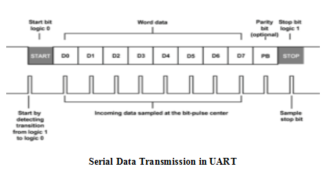
Serial Data Transmission in UART

Just because there is no clock signal a start bit is added sent first to tell the receiver to listen out for data. The receiver monitors for a logic HIGH falling to logic LOW. The receiver synchronizes its own bus clock to that make up the word being sent, with bit zero, the least significant bit (LSB) being sent first. The bits are sent as pulses on the wire at specific time intervals, set at both ends of links to previously agreed values. The receiver looks at the voltage on the wire at these times; if it sees logic high, it records a binary digit 1 or 0 if the line is low. The receiver checks half way between the start and the end of the pulse to ensure it does not miss-read the voltage on the line during the brief interval while the voltage is rising or falling.


If two devices use a parity bit for rudimentary error checking, that is calculated and sent next, in sync with data that has been transmitted thus far. Finally, one stop bit is sent by the transmitter. Word length, parity availability and type, and numbers of stop bits all have to be agreed in advance for successful communication because UART uses two wires. The transmitter of device-A connected to receiver of device-B and receiver of device-A connected to transmitter of device-B. This is how devices can send data simultaneously to each other, a mode of communication called ‘full duplex’.


UART is widely used serial communication protocol in embedded system based applications. Almost all microcontrollers have built-in on-chip UART support. LPC2148 ARM7 core supports two UART in it, UART0 and UART1. UART0 can be used as general purpose UART and also can support ISP Programming through it, whereas UART1 has additional modem support. Both have built in baud rate generator and 16-byte transmit and receive FIFOs. For UART0 the TxD Pin is at P0.0 and RxD Pin is at P0.1 and similarly for UART1 the TxD Pin is at P0.8 and RxD Pin is at P0.9 as shown in table below:


To communicate over UART or USART, we just need three basic signals which are namely, RXD (receive), TXD (transmit), GND (common ground). So to interface UART with LPC2148, we just need the basic signals. Display a text in PC using LPC2148 Development Board through UART module. In LPC2148 Development Board contains two serial interfaces that are UART0 & UART1. Here we are using UART0. The Transmitter pins send the data into PC and the receiver pin receives the data from PC. The PC and microcontroller speed are denoted by using baud rate. When the baud rates of both PC and Microcontroller are same, then only the data transmit and receive correctly otherwise not.

RS232 Level Converter

Most of microchips work on TTL or CMOS voltage level which can’t be used to communicate over RS-232 protocol. In this case voltage or level converter is needed which can convert TTL to RS-232 and RS-232 to TTL voltage levels. The most commonly used RS-232 level converter is MAX3232 chip. This chip includes charge pump which can generate RS232 voltage levels (-10V and +10V) from 5V power supply. It also includes two receiver and two transmitters and is capable of full-duplex UART communication. RS232 communication enables point-to-point data transfer, which often used in data acquisition applications and for data transfer between microcontroller and PC.

There are many registers to configure and initialize the UART, they are as follows:

• Control and Status Registers

• Data Related Registers

• Baud Rate Setup related registers 

• Interrupt Related Registers

Control and Status Registers :

1) U0FCR – FIFO Control Register : Used to control Rx/Tx FIFO operations.

1. Bit 0 – FIFO Enable : 1 to Enable both Rx and Tx FIFOs and 0 to disable.

2. Bit 1 – Rx FIFO Reset : Writing a 1 will clear and reset Rx FIFO.

3. Bit 2 – Tx FIFO Reset : Writing a 1 will clear and reset Tx FIFO.

4. Bits [7 to 6] : Used to determine that how many UART0 Rx FIFO characters must be written before an interrupt is activated.

[00] (i.e trigger level 0) for 1 character.

[01] (i.e trigger level 1) for 4 characters.

[10] (i.e trigger level 2) for 8 characters.

[11] (i.e trigger level 3) for 14 characters.

5. Others bits are reserved.

2) U0LCR – Line Control Register : Used to configure the UART block (i.e the data format used in transmission).

1. Bit [1 to 0] – Word Length Select : Used to select the length of an individual data chunk. [00] for 5 bit character length. Similarly [01] , [10] , [11] for 6 , 7 , 8 bit character lengths respectively.

2. Bit 2 – Stop bit select : 0 for using 1 stop bit and 1 for using 2 stop bits.

3. Bit 3 – Parity Enable : 0 to disabled Partiy generation & checking and 1 to enable it.

4. Bit [5 to 4] – Parity Select : [00] to Odd-parity , [01] for Even-parity , [10] for forced “1”(Mark) parity and [11] for forced “0”(Space) parity.

5. Bit 6 – Break Control : 0 to disable break transmission and 1 to enable it. TxD pin will be forced to logic 0 when this bit is 1.

6. Bit 7 – Divisior Latch Access bit : 0 to disable access to divisor latches and 1 to enable access.

3) U0LSR – Line Status Register : used to read the status of Rx and Tx blocks.

1. Bit 0 – Receiver Data Ready(RDR) : 0 means U0RBR is empty(i.e Rx FIFO is empty) and 1 means U0RBR contains valid data.

2. Bit 1 – Overrun Error(OE) : 0 means Overrun hasn’t occured and 1 means Overrun has occured. Overrun is the condition when RSR(Receive Shift Register)[See note 1] has new character assembled but the RBR FIFO is full and the new assembled character is eventually lost since no data is written into FIFO if its full. (Note: Reading U0LSR clears this bit)

3. Bit 2 – Parity Error(PE) : 0 mean no parity error and 1 mean a parity error has occured. When the value of the parity bit in the recieved character is in wrong state then a parity error occurs. (Note: Reading U0LSR clears this bit)

4. Bit 3 – Framing Error(FE) : 0 means no framing error has occured and 1 means that a framing error has taken place. Framing error occurs when the stop bit of a received character is zero. (Note: Reading U0LSR clears this bit)

5. Bit 4 – Break Interrupt : 0 means no Break Interrupt occures and 1 means that it has occured. A Break Interrupt occurs when the RxD line is pulled low (i.e all 0s) i.e held in spacing state for 1 full character after which Rx Block goes into Idle state. Rx Block gets back to active state when RxD pin is pulled high (i.e all 1s) i.e held in marking state for 1 full character. (Note: Reading U0LSR clears this bit)

6. Bit 5 – Transmit Holding Register Empty(THRE) : 0 means U0THR contains valid data and 1 means its empty.

7. Bit 6 – Transmitter Empty (TEMT) : 0 means U0THR and/or U0RSR contains valid data and 1 means that both U0THR and U0RSR are empty.

8. Bit 7 – Error in RX FIFO(RXFE) : 0 means that U0RBR has no Rx Errors or Rx FIFO is disabled(i.e 0th bit in U0FCR is 0) and 1 means that U0RBR has atleast one error.

4) U0TER – Transmit Enable Register : This register is used to enable UART transmission. When bit-7 (i.e TXEN) is set to 1 Tx block will be enabled and will keep on transmitting data as soon as its ready. If bit-7 is set to 0 then Tx will stop transmission. Other bits are reserved.

Data Related Registers :

1) U0RBR – Receiver Buffer Register (READ ONLY!): This register contains the top most byte(8-bit data chunk) in the Rx FIFO i.e the oldest received data in FIFO. To properly read data from U0RBR , the DLAB(Divisor Latch Access) bit in U0LCR register must be first set to 0. Also , as per the user manual “The right approach for fetching the valid pair of received byte and its status bits is first to read the content of the U0LSR register, and then to read a byte from the U0RBR.

2) U0THR – Transmit Holding Register (WRITE ONLY!): U0THR contains the top most byte in Tx FIFO and in this case its the newest(latest) transmitted data. As in the case with U0RBR , we must set DLAB=0 to access U0THR for write operation.

Baud Rate Setup related registers :

1) U0DLL and U0DLM – Divisor Latch registers: Both of them hold 8-bit values. These register together form a 16-bit divisor value which is used in baud rate generation which we will see in later section. U0DLM holds the upper 8-bits and U0DLL holds the lower 8-bits and the formation is “[U0DLM:U0DLL]“. Since these form a divisor value and division by zero is invalid, the starting value for U0DLL is 0x01 (and not 0x00) i.e the starting value in combined formation is “[0x00:0x01]” i.e 0x0001. Please keep this in mind while doing baud-rate calculations. In order to access and use these registers properly, DLAB bit in U0LCR must be first set to 1.

2) U0FDR – Fractional Divider Register : This register is used to set the prescale value for baud rate generation. The input clock is the peripheral clock and output is the desired clock defined by this register. This register actually holds to different 4-bit values (a divisor and a multiplier) for prescaling which are:

1. Bit [3 to 0] – DIVADDVAL : This is the prescale divisor value. If this value if 0 then fractional baud rate generator wont have any effect on Uart Baud rate.

2. Bit [7 to 4] – MULVAL : This is prescale multiplier value. Even if fractional baud rate generator is not used the value in this register must be more than or equal to 1 else UART0 will not operate properly.

3. Other Bits reserved.

Interrupt Related Registers :

1) U0IER – Interrupt Enable Register: Set a bit to 0 to disable and 1 to enable the corresponding interrupt.

1. Bit 0 – RBR Interrupt Enable

2. Bit 1 – THRE Interrupt Enable

3. Bit 2 – RX Line Status Interrupt Enable

4. Bit 3 – ATBOInt Enable

5. Bit 4 – ATEOInt Enable

Where ATBOInt = Auto Baud Time-Out Interrupt , ATEO = End of Auto Baud Interrupt and rest of the bits are reserved.

2) U0IIR – Interrupt Identification Register: Refer User Manual when in doubt. In some application the usage of this register might get a bit complicated.

This register is organized as follows:

1. Bit 0 – Interrupt Pending : 0 means atleast one interrupt is pending , 1 means no interrupts are pending. Note: This bit is ACTIVE LOW.

2. Bits [3 to 1] – Interrupt Identification : [011] is for Receive Line Status(RLS) , [010] means Receive Data Available(RDA) , 110 is for Character Time-out Indicator(CTI) , [001] is for THRE Interrupt.

3. Bits [7 to 6] – FIFO Enable.

4. Bit 8 – ABEOInt : 1 means Auto Baud Interrupt has successfully ended and 0 otherwise.

5. Bit 9 – ABTOInt : 1 means Auto Baud Interrupt has Timed-out.

6. All others bits are reserved.

Programming Steps

• Initialize the LCD

• Initialize the Serial Communication (9600 BaudRate)

• Receive the 12 bytes and display it into the LCD Display

Application

• GPS

• Wireless communication

• Modem

• Bluetooth modules

Proteus design for UART interfacing with ARM


Orcad design for UART interfacing with ARM


UART interfacing with ARM

/*  Name     : main.c
 *  Purpose  : Source code for UART Interfacing with ARM LPC2148.
 *  Author   : Gemicates
 *  Date     : 2018-02-02
 *  Website  : www.gemicates.org
 *  Revision : None
 */
#include <lpc214x.h>      			  		 // header file for LPC21XX series

void ser_init(void);
void tx(unsigned char c);
unsigned char rx(void);
void tx_string(unsigned char *s);


void main()	                                                 // main function
{
 ser_init();
 tx('S');
 }
 void ser_init()                                                 // Funtion to Initialize UART
{
 VPBDIV=0x02;                                                    // PCLK = 30MHz
 PINSEL0|=0x05;
 U0LCR=0x83;
 U0DLL=195;
 U0DLM=0;
 U0LCR=0x03;
 U0TER=(1<<7);
}
 
void tx(unsigned char c)                                         // Funtion to transmit the data
{
 U0THR=c;
 while((U0LSR&(1<<5))==0);
}
 
void tx_string(unsigned char *s)
{
 while(*s) {
 tx(*s++);
 }
}
 
unsigned char rx()                                               // Funtion to recive the data
{
 while((U0LSR&(1<<0))==0);
 return U0RBR;
}   

Error message here!

Show Error message here!


Forgot your password?

Error message here!

Send OTP

Error message here!

Show Error message here!


Lost your password? Please enter your email address. You will receive a password you Need.

Send Error message here!


Back to log-in

Close